Technology
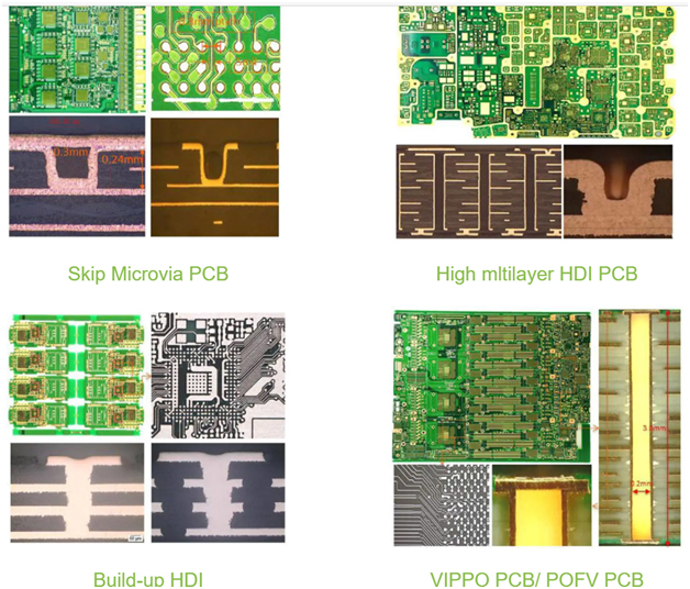
Advanced HDI / Aluminum Substrate / Copper Coin
HDI PCB fabrication is one of our core competencies at PROTOPCB. We have the equipment, people, engineering expertise, certifications, and track record to meet the most demanding requirements of HDI PCB fabrication. Our extensive PCB manufacturing capabilities support the most challenging requirements for advanced HDI PCB designs in all industries, including medical, aerospace, defense, communications and commercial markets among others.
We support up to 40 laminates, laser drilling, micro via holes, stacked micro via holes, blind holes, buried through holes, via- in-pads, laser direct imaging, sequential lamination, 00175 “trace/space, controlled impedance among many other attributes.
PROTOPCB produces HDI PCB’s without any minimum order requirements while offering the most flexible turnaround time options. Each design is reviewed in detail by our front-end engineering and cam planningexperts. This ensures the addressing of all issues prior to the manufacturing process. Our world class customer service and engineering group support team is available 24 hours a day to assist with your HDI PCB fabrication requirements.
HDI boards have an inner and an outer circuitry, and then the use of High technology drilling and metallization in the hole to realize the internal connection of each layer circuit. Generally, build-up manufacturing is used. The more times of lamination, the higher the technical grade of the board. The common HDI board is basically a one-time build-up, and the high-stage HDI adopts two or more times of lamination technology and adopts advanced PCB technologies such as stack hole, electroplating hole filling, laser direct drilling, etc. With the development of science and technology, electronic design is constantly improving the performance of the whole machine, but also trying to reduce the size. From mobile phones to smart weapons, “small” is the eternal pursuit. High-density integration (HDI) technology can make the design of terminal products more miniaturized and meet the higher standards of electronic performance and efficiency.
Typical features of HDI PCB
The micro blind hole ring is less than 6mil the wiring line width between inner and outer layers is less than 4mil and the pad diameter is no more than 0. 35mm.
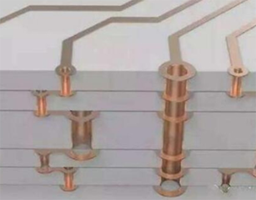
- Blind hole: which connects the inner layer with the outer layer.
- Buried hole: which realizes the connection between the inner layer and inner layer.
All of them are small holes with a diameter of 0. 05mm ~ 0. 15mm. There are laser drilling, plasma etching, and photo-induced drilling. Laser drilling is usually used, and laser drilling is divided into CO2 and YAG ultraviolet laser (UV).
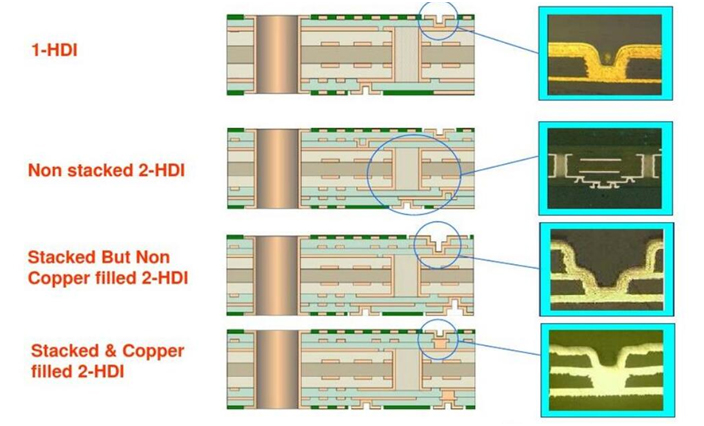
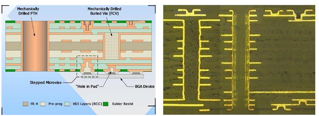
In the 6 layer laminate, the first stage and the second stages are for the board to be laser drilled.
The first stage HDI board(1+N+1 HDI) refers to,
Blind hole: 1-2, 2-5, 5-6, that is, 1-2, 5-6 need laser drilling.1`
Two-stage HDI PCB (2+N+2 HDI ) refers to,
Blind hole: 1-2, 2-3, 3-4, 4-5, 5-6. First drill 3-4 buried holes, then laminate 2-5, then drill 2-3, 4-5 laser holes for the first time, press 1-6 for the second time, and then drill 1-2, 5-6 laser holes for the second time. Finally, the through-hole was drilled. It can be seen that the 2-stage HDI PCB has been pressed twice and laser-drilled twice.
In addition, the 2-stage HDI board can also be divided into staggered via 2-stage HDI board and stack via 2-stage HDI board. Staggered hole 2-stage HDI board means that blind holes 1-2 and 2-3 are staggered, while stacked hole 2-stage HDI board refers to blind holes 1-2 and 2-3 stacked together, such as blind: 1-3, 3-4, 4-6. So on, the 3-stage and 4-stage are the same.
Advantages of HDI PCB’s
The cost of PCB can be reduced: when the density of PCB increases more than eight layers, the cost of HDI manufacturing will be lower than that of the traditional complex lamination process.Increase line density: interconnection between the traditional circuit board and partsIt is conducive to the use of advanced construction technologyBetter electrical performance and signal accuracyGood reliabilityIt can improve the thermal propertiesIt can improve radio frequency interference / electromagnetic wave interference / electrostatic discharge (RFI / EMI / ESD)Increase design efficiency
Material of HDI PCB
Some new requirements for HDI PCB materials are proposed, including better dimensional stability, antistatic mobility, and nonadhesive. The typical material of HDI PCB is RCC (resin-coated copper). RCC has three types, namely polyimide metalized film, pure polyimide film, and cast polyimide film.
Advantages of RCC include small thickness, lightweight, flexibility and flammability, compatibility characteristic impedance, and excellent dimensional stability. In the process of HDI Multilayer PCB, the traditional adhesive chip and copper foil can be replaced as the insulating medium and conductive layer. The traditional suppression technology can be used to suppress RCC. Nonmechanical drilling methods such as lasers are then used to form micro through-hole interconnections.
RCC promotes the emergence and development of PCB products from SMT (surface mounting technology) to CSP (chip-level packaging), from mechanical drilling to laser drilling, and promotes the development and progress of PCB micro through holes. All of this makes RCC the leading HDI PCB material.
In the actual PCB manufacturing process, there are usually FR-4 standard TG 140C, FR-4 high Tg 170C, and FR-4 and Rogers combination lamination, which are mostly used now. With the development of HDI technology, HDI PCB materials must meet more requirements, so the main trend of HDI PCB materials should be:
- Development and application of flexible materials without binder;
- The thickness of the dielectric layer is small, and the deviation is small;
- The development of LPIC;
- The dielectric constant becomes smaller and smaller.
- The dielectric loss is getting smaller and smaller.
- High welding stability;
- Strictly compatible with CTE (coefficient of thermal expansion);
Material of HDI PCB
Unique HDI PCB manufacturing lies in micro hole manufacturing, through-hole metallization and thin wire.
Micro-via hole manufacturing
Micro via manufacturing has always been the core issue of HDI PCB manufacturing. There are two main drilling methods:
- For ordinary through-hole drilling, mechanical drilling is always the best choice for its high efficiency and low cost.
- There are two types of laser drilling: photothermal ablation and photochemical ablation. The former refers to the process of heating the operating material after high energy absorption of laser to make it melt and evaporate through the formed through-hole. The latter refers to the results of high-energy photon and laser length exceeding 400 nm in the ultraviolet region.
- There are three types of laser systems for the flex-rigid board: excimer laser, UV laser drilling, CO2 laser. Laser technology is not only suitable for drilling, but also suitable for cutting and forming. Although the cost of laser drilling equipment is high, they have higher precision, stable technology, and mature technology. The advantages of laser technology make it the most commonly used method in blind / buried hole manufacturing. Today, 99% of HDI micro via holes are obtained by laser drilling.
Through-hole metallization
The biggest difficulty of through-hole metallization is the difficulty of uniform plating. For the deep hole electroplating technology of micro through-hole, in addition to using electroplating solution with high dispersion ability, the plating solution on electroplating device should be upgraded in time, which can be achieved by strong mechanical stirring or vibration, ultrasonic stirring, and horizontal spraying. In addition, the humidity of the through-hole wall must be increased before electroplating.
In addition to the process improvement, HDI through-hole metallization method also saw the main technical improvements: electroless plating additive technology, direct plating technology, etc.
Thin line
The realization of the thin lines includes traditional image transmission and laser direct imaging.
For laser direct imaging, there is no need for photographic film, and the image is directly formed on the photosensitive film by laser. UV wave lamp is used for the operation to avoid adverse effects caused by film defects. It can be directly connected to CAD / CAM to shorten the manufacturing cycle and make it suitable for limited and multiple small batches.
Aluminum PCB
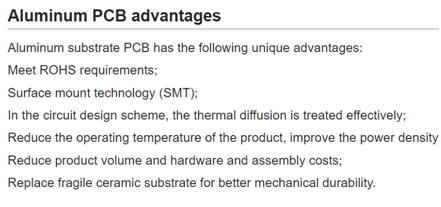
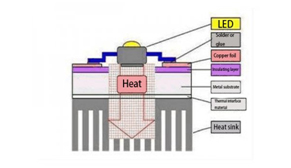
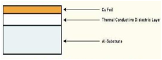
Aluminum Materials
The commonly used metal aluminum base boards for aluminum substrate mainly include 1000 series, 5000 Series and 6000 series. The basic characteristics of these three series aluminum materials are as follows:
- 1000 series represents 1050, 1060, 10701000 series aluminum plate, also known as pure aluminum plate. In all series, 1000 series has the most aluminum content, and the purity can reach more than 99. 00%. Because it does not contain other technical elements, the production process is relatively simple and the price is relatively cheap. It is the most commonly used series in conventional industries. Most of the 1050 and 1060 series are in circulation on the market. 1000 series aluminum plate is based on the last two digits to determine the minimum aluminum content of this series. For example, the last two digits of 1050 series are 50. According to the international brand naming principle, its aluminum content must reach 99. 5%, and the top is the qualified product. In China’s aluminum alloy technical standard (GB / t3880-2006), the aluminum content of 1050 is 99. 5%. In the same way, the aluminum content of 1060 series aluminum plate must reach more than 99. 6%.
- 5000 series represents 5052, 5005, 5083, 5A05 series. 5000 series aluminum plate belongs to the common alloy aluminum plate series, the main element is magnesium, the magnesium content is between 3-5%, which is also known as aluminum magnesium alloy. Its main characteristics are low density, high tensile strength and high elongation. In the same area, the weight of aluminum magnesium alloy is lower than other series, so it is often used in aviation, such as aircraft fuel tank. In addition, it is widely used in conventional industry. Its processing technology is continuous casting and rolling, belonging to the hot rolling aluminum plate series, so it can do oxidation deep processing.
- 6000 series represents 6061, which mainly contains magnesium and silicon. Therefore, it concentrates the advantages of 4000 series and 5000 series. 6061 is a cold-treated aluminum forging product, which is suitable for applications requiring high corrosion resistance and oxidation resistance. Good usability, excellent interface characteristics, easy coating and good processability.
- 6061General characteristics of: excellent interface characteristics, easy coating, high strength, good usability, strong corrosion resistance. Typical uses of 6061 aluminum: aircraft parts, camera parts, couplers, ship accessories and hardware, electronic accessories and joints. Considering the material's texture, hardness, elongation, chemical properties and price, 5052 aluminum plate is commonly used in 5000 series aluminum materials.
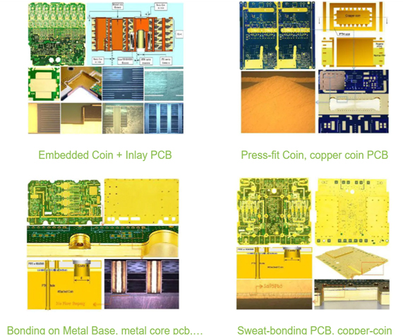
Press-fit Coin embedded PCB
With the development of new generation information technology, energy saving and new energy vehicles, electric power equipment,aerospace and other fields, the solution of heat dissipation problem is imminent. At present, there are many ways to solve the problem of PCBheat dissipation, such as dense heat dissipation hole design, thick copper foil circuit, metal-based (core) structure, embedded copper coindesign, copper-based convex design, high thermal conductivity materials and so on. Embedding copper in PCB directly is one of the effective ways to solve the problem of heat dissipation.
Embedded copper printed circuit boards (PCBs) have the characteristics of high thermal conductivity, high heat dissipation and space saving,which can effectively solve the heat dissipation problem of high-power electronic components.
Flex/Rigid Flex/Backplane/High Frequency
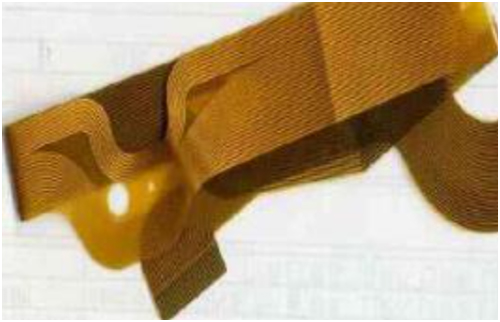
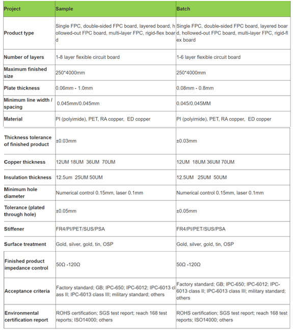
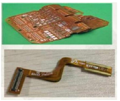
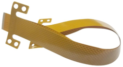
FLEX PCB
A copper trace pattern bonded or not using a flexible covering layer on a flexible substrate is called Flex PCB. These flexible circuits can be manufactured using the same components used to make rigid electronic circuits, the only difference being that the flexible circuits can be made into any desired shape according to the packaging of the product without affecting the connectivity.FLEX PCBs has the advantages of high wiring density, lightweight, thin thickness, less wiring space limitation, and high flexibility. It fully conforms to the development trend of light and short electronic products and is an effective solution to meet the requirements of miniaturization and mobility of electronic products.
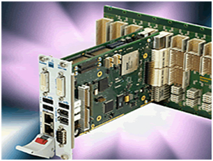
Backplanes
Backplane Application
Backplane applications are very wide, ranging from communication equipment, servers, medical equipment, large-scale machinery and aviation equipment need backplane PCB, to computers, servers and other integrated intelligent electronic devices, also need to organically coordinate various functional modules through the backplane PCB to achieve better system performance.
Size
A large part of the backplane is connected to some of the other boards at right angles. This requires that the backplane be much larger than conventional PCBs and that some backplanes even reach the 762mmx1066. 8mm
The number of layers
In terms of the most common backplane, its layer is already in the 16~28, this number is much higher than the ordinary PCB
Thickness
From the structure of the backplane itself, in order to be able to withstand more mechanical stress, it has to be designed much thicker than ordinary PCB. In most cases, the designer has to increase its thickness, and the typical backplane thickness is 2mm-4mm, which can be as thick as 4mm-6mm.
With the continuous development of science and technology, users of bandwidth requirements are becoming more and more stringent, which requires that the design of the backplane to be precise and rigorous enough, the production process of ordinary PCB has been far from meeting the needs of modern production. In order to produce a backplane that meets a variety of conditions, it is necessary to eliminate some of the original conventional equipment and replace it with a hybrid bus structure and assembly technology.
What’s the key points of Backplane Technology
In order to achieve high performance requirements, PCB manufacturing must face the challenges of strict plate thickness, board size, number of layers, alignment control, back drilling depth and stub line. In backplane manufacturing, all the aspects mentioned below are key issues.
Alignment control
Due to more and more layers required by users, the alignment between layers becomes very important. Alignment control is the most important manufacturing problem for ultra Multilayer PCB manufacturing, because poor alignment control may lead to short circuit.
Alignment control is affected by many programs and elements, of which cascade is the most important. Tolerance convergence is required for interlayer alignment. The change of plate size makes the convergence more demanding. All layout processes are generated in a certain temperature and humidity controlled environment. When the exposure equipment is in the same environment, the alignment tolerance of the front and back images of the whole area should be kept at 0. 0125 mm, and CCD camera should be used to complete the front and back layout alignment. After etching, the inner laminate is perforated using a four hole system. Through the core plate, the position accuracy is 0. 025mm, and the repeatability is 0. 0125mm. Then the pin is inserted into the perforation to align the etched inner layers and bond the inner layers together. Using this method, the hole can be fully aligned with the etched copper plate to form a solid annular design structure. However, in order to keep the fixed cost of PCB unchanged, the etching copper plate size is required to be smaller, so the interlayer copper plate is required to be better aligned. Fixtures and conveying equipment must be able to transfer large and heavy plates simultaneously
Protopcb’s long established backplane manufacturing history dates back to the 1970’s. we’ve been providing the most advanced backplanes to the most prolific telecommunications companies. oems have relied on our stellar performance and service without us losing even one account for any quality, delivery, value or any other issue except for the oem company transitioning out of the business.
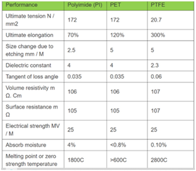
High Frequency PCB’S
High frequency PCBsare widely used in RF and Microwave PCB. High frequency PCB materials are different from conventional FR4 materials. Most of them use PTFE &Teflon materials. Good electrical properties and low signal loss are the basis.choose Rogers dielectric material because of its lower dielectric and signal loss, lower circuit manufacturing cost, and more suitable for rapid turnover prototype application.In addition to selecting the right PCB material and determining the correct Er value, the designer should also consider the conductor width and spacing, substrate constant, and other parameters. The highest level of process control must be used to specify and implement these parameters precisely.High frequency PCB board (HF PCB) refers to the special circuit board with high electromagnetic frequency, which is used for high frequency (frequency greater than 300MHz or wavelength less than 1m). Generally speaking, high frequency board can be defined as a circuit board with a frequency above 1GHz. Substrate materials need to have excellent electrical properties and good chemical stability. With the increase of power signal frequency, the loss requirement on the substrate is very small, so the importance of high-frequency material is highlighted. SEE OUR MATERIALS PAGE FOR HIGH REL FREQUENCY MENU