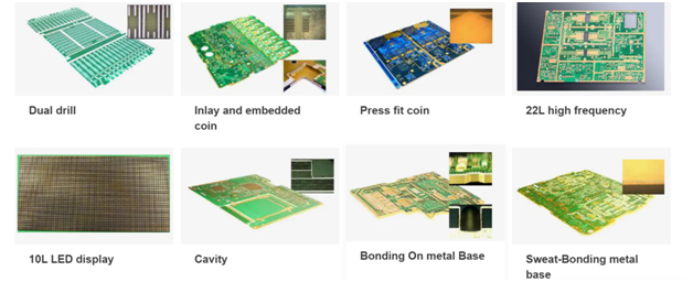
Capabilities
Trace/Holes/Layers/Materials/Surface Finish/Heavy CU
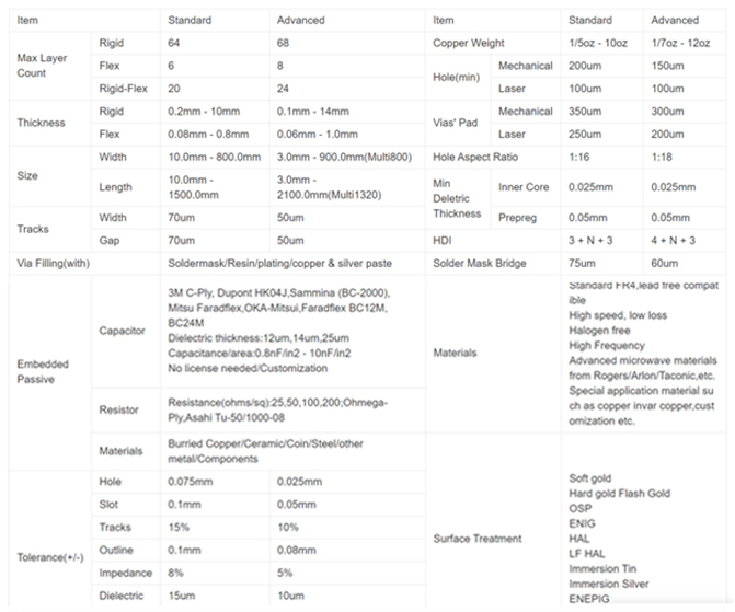
PROTOPCB is capable of almost any PCB fabrication. Check our capabilities. Up to 64 layers, RIGID, FLEX, RIGID FLEX, board thickness 10 mm, min line width/space 1.5/1.5 mil, min hole 0.2 mm, laser hole 3 mil, 4+N+4 HDI, POFV, via filling with copper, high-speed and high-frequency,abundant materials, impedance tolerance 5-10%, most popular surface treatments. See the following capabilities in more detail:
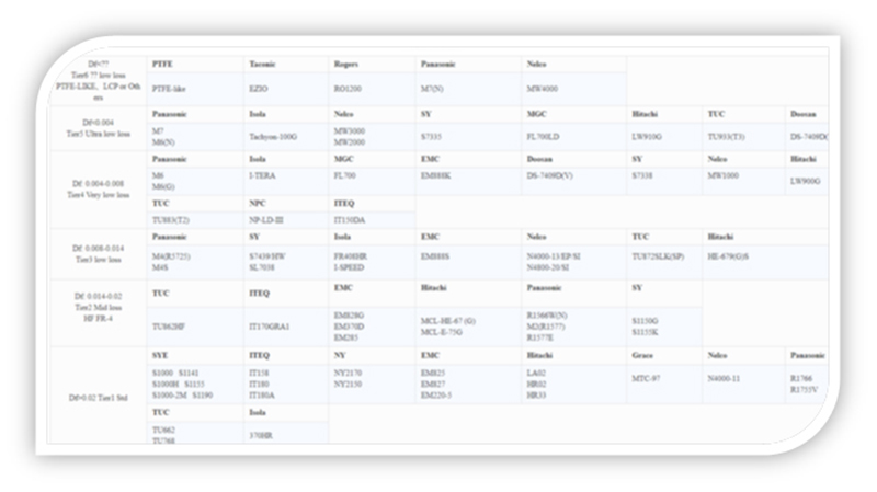
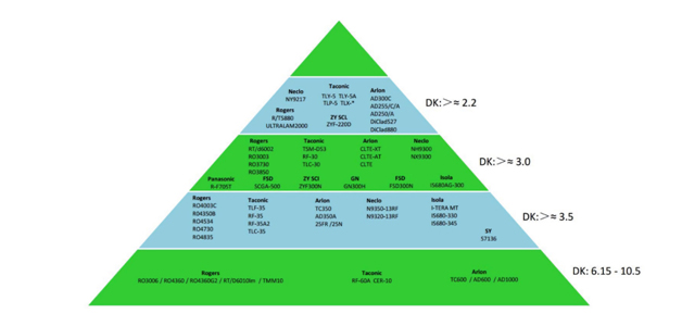
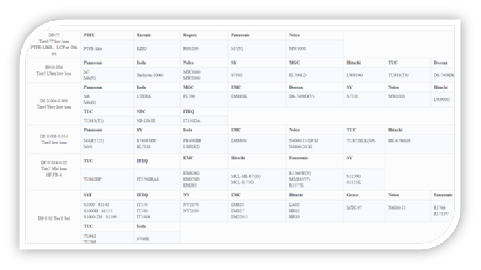
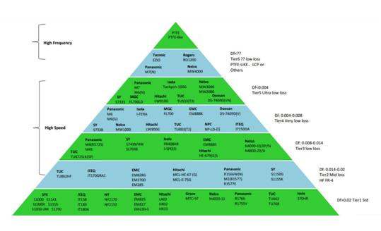
PCB MATERIALS
Broadest Range OF Laminate Types
PROTOPCB offers customers one of the largest Laminate portfolios in the PCB Industry. Our In-stock availability facilitates complete continuity in your TIME CRITICAL projects. Material types including PTFE, high speed/low loss, high temperature, low CTE, lead-free types, etc. We also offer RF/digital hybrid construction, combination surface finishes,stacked/staggered solid copper-filled micro vias, foam-bonded structures and numerous surface finishes, including ENIPIG, ENIG, HASL, Sn/Pb reflow, silver, and tin.For a complete list of laminate materials, please view our PCB Materials Guide. More details? Contact us.
Combining High Performance with Manufacturability
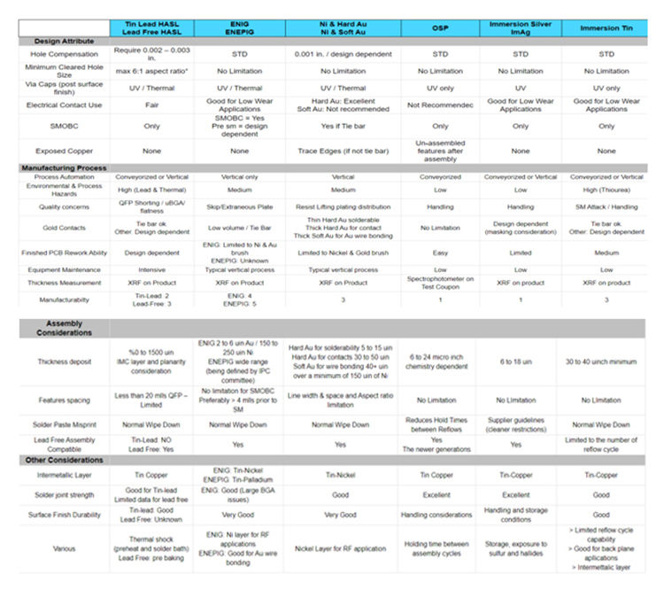
PrototypePCB provides many different PCB surfaces finishes for a variety of applications. Our engineering teams and technical staff can assist in the selection of materials based on requirements throughout the DFM process.
Surface Finish Options
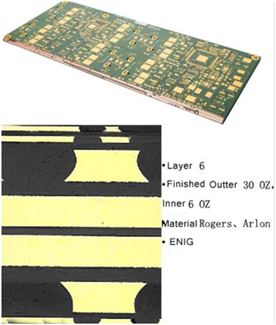
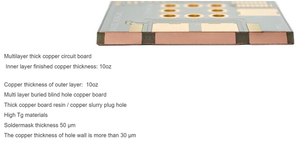
Heavy/Thick Copper PCBs
High-power, high current server power supply boards and other PCB high CU demandsthese power boards need high heat resistance, high heat dissipation and other characteristics. Due to the thick copper (≥ 3oz) characteristics of thick copper PCBs, there can bemanufacturing nuances , especially in the lamination process where there is large copper free areas. These cavities and their uneven thickness, can put limitation in PP selection, matching of lamination program, temperature rise and vacuum capacity of the laminator, the solution of the inner layer glue (flow glue route), residual copper rate control, withstanding voltage requirements, the main points of thick copper PCB engineering, the treatment of circuit coils, multiple electroplating, multiple solder masks, etc. are all better in the hands of experienced proceesing experts. PROTOPCB provides prototyping and solves these processing services for thick copper PCBs.
In the PCB industry, there is no clear definition of thick copper PCB boards& heavy copper PCBs & power supply PCBs. The copper foil with nominal thickness of more than 105 μm is generally referred to as thick copper foil. Most circuit boards use 35um copper foil thickness, which mainly depends on PCB usage and signal voltage / current. For PCB with excessive current, some of them will use 70UM copper thickness, 105um copper thickness, and rarely 140um copper thickness.The average current of the signal is large, the current that can be carried by the wiring width should be considered. The line width can refer to the thickness of copper foil in PCB design.
Generally, the copper thickness of the finished product of 2oz, the silk screen printing by hand is not enough to fill the gullies between the lines, so the solder mask must be printed twice.
Therefore, the circuit board process for 2oz and thicker always calls out on the Traveler: thick copper board, needs2x soldermask. The effect that the line doesn’t turn red and the thickness of the soldermask on the line surface is greater than 10um.
Copper plating usually includes primary copper and secondary copper. The main purpose of primary copper is to provide sufficient copper thickness for secondary copper etching, so as to ensure that the copper thickness after secondary copper etching can meet the customer’s standard requirements.Thick copper circuit boards can generally process 6oz, 3oz thick copper board, generally need multi-layer screen printing and multi-layer solder mask and multi-layer copper deposition to meet customer needs.
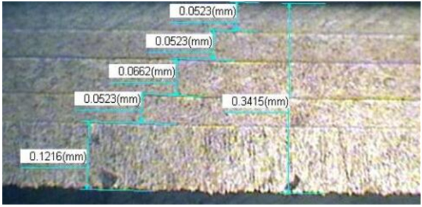
10 oz copper circuit metallographic section(secondary dry film method by LDI, 4 times plating)