State of Art Facilities
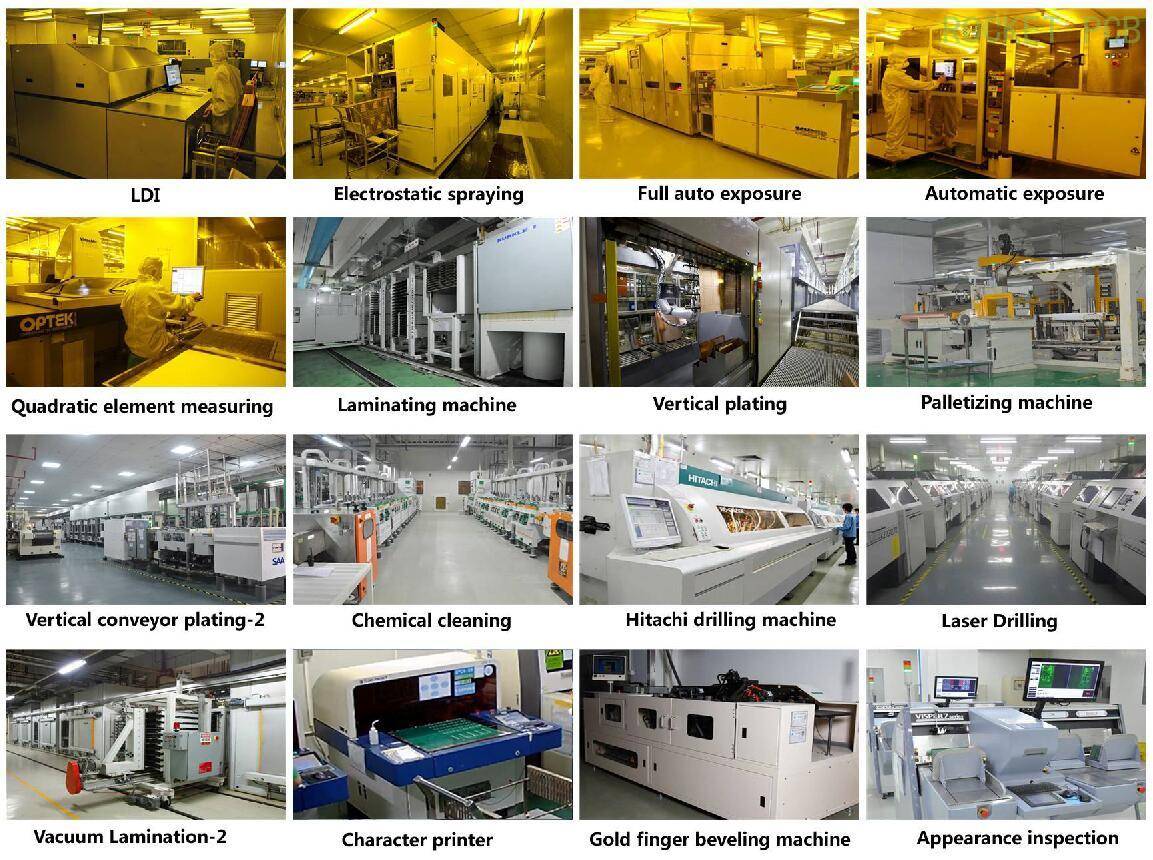
State of the Art PCB Equipment& Facilities
PROTOPCB has amassed the most advanced PCB Manufacturing equipment available. This enables us to take on the most advanced PCB manufacturing builds in the industry. Technology ranging from Advanced HDI PCB’s, RF PCBs, Hybrid PCBs, Backplane PCBs, Embedded PCBs, High Layer PCBs, High Rel & Frequency PCBs. OEMs require a Printed Circuit Manufacturing partners capabilities and successful performance to leverage their NPI launches with utmost quality,especially in “Time Critical” windows. PROTOPCB’s equipment redundancy and parallel processing negates manufacturing interruptions and delays. Job flow continuity is at the core of our competencies in the highest of standards of PCB manufacturing. This all serves to deliver on customer expectations. For almost 50 years PROTOPCB continues to invest among the highest industry profit re-investment in its’ “State of the Art Facilities. PROTOPCB believes this investment yields the highest possible return;
TOTAL CUSTOMER SATISFACTION.
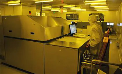
LDI Exposure Machine
Compared with the traditional CCD semi-automatic exposure machine, LDI has many advantages, such as no need for direct imaging of film, reducing the cost of film production, shortening the sample delivery time, reducing the error of film production and alignment, and more accurate circuit exposure. In addition to the above advantages, the exposure speed of LDI is slower than that of CCD, but it is indispensable for making high-precision circuits.
Electrostatic Spraying
For the spray technology of solder resist ink, there are screen printing, electrostatic spray, low-pressure spray and other technologies. Screen printing requires a large number of skilled screen printing talents, which is the most ink saving coating method; automatic screen printing machine, which is suitable for large quantities of pcb boards. Electrostatic spraying technology is very mature, which can save a lot of manpower. The PCB prototype and batch boards are applicable, but there are also shortcomings: large ink consumption, relatively expensive equipment, and high maintenance costs.
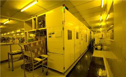
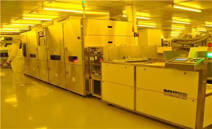
Automatic Exposure Machine
The production of PCB originally used printing to draw the circuit diagram on the PCB. Now it is mainly made by scattering light source exposure machine or parallel light source exposure machine. In the traditional manual exposure machine, the whole process is completed manually, and the alignment accuracy is judged by human eyes. The batch alignment accuracy is generally maintained at ± 50 μm. At present, PCB has developed towards the direction of high precision, small aperture and multi-layer. The requirement for position accuracy is up to ± 10 μm, which has exceeded the limit of human eye resolution. Therefore, the requirements for PCB manufacturing and testing equipment will be more and more stringent. The semi-automatic and full-automatic exposure machine adopts the CCD visual automatic alignment technology, which has the advantages of fast alignment speed, high alignment accuracy and good product consistency, and meets the requirements of such high-precision alignment.
Vacuum Laminator
It is used for lamination of multi-layer boards with more than 4 layers. Lamination is the key process for making multi-layer boards. Whether there is a large laminating machine is the embodiment of the factory’s strength. Generally, only a large PCB factory has the ability to produce multi-layer boards and ultra multi-layer circuit boards.
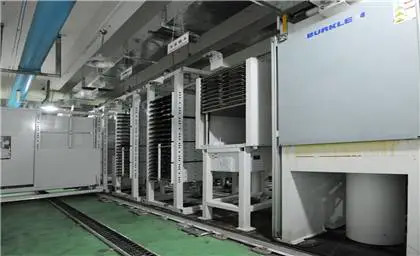
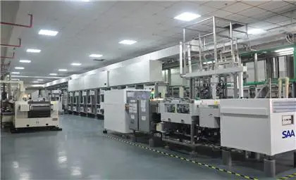
VCP vs Hoist Type Plating
Vertical continuous plating, used in PCB copper plating, using spray copper plating process and vertical continuous conveyor of the whole board (one time) copper plating production line.
There are many advantages compared with the traditional hoist type plating: stable plating efficiency — all workpieces are continuously moved from one side of the plating to the other side, and the production conditions of each workpiece are exactly the same.
It has better deep plating ability and the thickness diameter ratio can reach 12:1.
Better uniformity of copper plating, saving equipment consumables, such as phosphor copper ball, water and electricity costs, saving labor, equipment maintenance costs, etc
Laser Drilling Machine
CO2 laser is widely used in the production of industrial micro through holes of printed circuit board, and the diameter of micro through holes should be greater than 100 μm. CO2 laser has a high productivity in the production of these holes, which is due to the short drilling time required for CO2 laser. UV laser drilling technology is widely used in the production of micro holes with diameter less than 100 μm, with the application of micro circuit diagram, the hole size can be even less than 50 μm. The output of ultra violet laser is very high when it is used to make holes with diameter less than 80 μm. Therefore, in order to meet the need of increasing microvia productivity, many PCB manufacturers have begun to introduce double head laser drilling system.
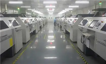
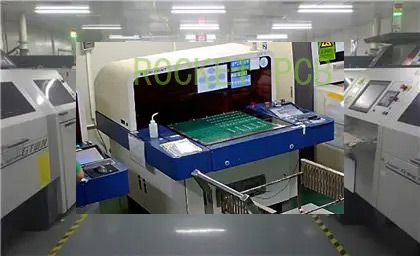
Character Printer
It is suitable for PCB character spray printing. It can replace traditional silkscreen printing and provide PCB manufacturer with a set of high precision, high quality and high efficiency spray printing production solution. Short production cycle, no need to make the silk screen, good printing stability, high quality, high printing accuracy, saving labor costs.
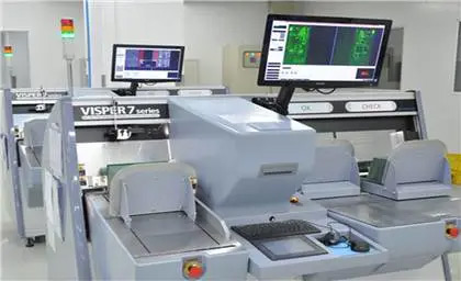
Appearance Visual Inspection
At present, some PCB manufacturers still use the traditional manual visual inspection method. However, the manual visual inspection itself has some defects, and with the improvement of production output and quality demand, the manual visual inspection obviously can not meet the demand, which requires the use of an appearance inspection machine. Especially for the circuit board factory with low replacement frequency and mass PCB production.
Appearance inspection machine can effectively detect small defects such as finger print, exposed copper of circuit, exposed copper of base material, excessive etching, sundries on pad, board damage, oil stain, scratch, glue stain, character overprint, character on pad, too thin soldermask, ink on pad , unclear characters, etc. it is an effective way for circuit board factory to improve quality and output.
